Reconfigurable field effect transistors (RFET) is expected to offer a lower transistor count and decreased area consumption compared to conventional CMOS. While the semiconductor industry is moving towards sub-10nm transistor technologies, silicon nanowires are considered a major evolutionary step for FinFET technology due to their outstanding electrostatic control over the channel. The first use of SiNW for implementing reconfigurable transistors was demonstrated in 2012. However, a key advantage of SiNW RFET is logic reconfigurability at the device level. Conventional CMOS relies on fixed PMOS and NMOS transistors that respectively operate p- (holes being the charge carriers) and n-type (electrons carrying charge) channels. A single SiNW RFET device, however, can be configured to operate with n- or p-type channels at runtime. This fine-grain reconfigurability enables the circuit to realize multiple functionalities depending on the configuration of the devices.
Compatibility with the CMOS Fabrication Process
SiNW RFET relies on a CMOS-compatible process for fabrication. One main advantage is that the SiNW RFET process does not require chemical doping, but instead fully relies on electrostatic doping to operate. A promising structure for implementing SiNW RFETs is the three-independent gate field-effect transistor (TIGFET) that comprises three gates. As shown in Figure 1, the device channel is formed by silicon nanowires connecting the metallic source (S) and drain (D) pillars. Three gates are placed on the nanowires that are named with respect to their distances from the source and drain. The middle gate is called the control gate (CG), the polarity gate-drain (PGD) gate is closer to drain, and the polarity gate-source (PGS) is closer to the source. Two modes of operation are possible based on the voltage bias between the source and drain. CG controls the potential barrier in the device, which toggles the device between the ON and OFF states. The bias between PGS and PGD defines the mode of operation for the device (p-channel or n-channel). A positive PGS-PGD bias enables electron conduction at the source-drain junctions, setting the device polarity to n-type; whereas, a low PGS-PGD bias enables hole conduction at the Schottky barriers, setting the device to p-type.

Figure 1. A conceptual sketch of a vertically-stacked nanowire TIGFET.
Basic Capabilities of TIGFET Circuits
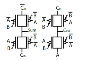
A TIGFET device can be conceptually seen like a conventional CMOS device with an extra terminal, called polarity gate, which sets the device into either its n- or p-channel modes. This unique capability can be exploited to design circuits with superior capabilities, such as a 3-input majority vote (3-MAJ) and a 3-input exclusive-OR (3-XOR). Figure 2 illustrates a full-adder implementation with TIGFETs. The Sum and Cout circuits have 4 transistors each, which gives it the same complexity as a CMOS NAND circuit, enabling exciting opportunities to design arithmetic logic at the same cost as control logic.

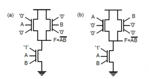
Moreover, TIGFETs also enable more powerful multi-VT circuit design than CMOS. Figure 3 gives an example of a NAND gate implemented in either Low-Leakage or High-Performance modes. Both variations of the design use the exact same TIGFET technology. Therefore, with TIGFET, the VT selection now comes as a design and routing knob, and not anymore as a technology option.

Applications and Implications for Computer Architects
Low power is a very crucial factor in current IC/SoC designs given the recent trends in technology scaling. For each improvement in technology node size, the corresponding increase in dynamic and leakage current density completely overshadows the minimal improvement in speed. As seen above, in TIGFET, the threshold control is done by selecting which gate to use on the device. Unlike CMOS, TIGFET does not trade-off the leakage reduction with the ON-state current. This helps TIGFET to achieve dual VT performance at a reduction of loss in performance. This may hold much interest for computer architects especially when low power/high-performance circuits have to be designed, where the architect can achieve the lowest power consumption possible for an application without trading off the performance by too much, and it simplifies the technology massively.
Hardware security is another important area of focus for computer architects, especially since the expose of the Spectre and Meltdown attacks. TIGFET has great potential towards no-/low-overhead techniques for protection of circuit designs and IP cores and protection against counterfeit ICs (e.g., secure circuits, differential power analysis mitigation, and physically unclonable functions). Some case studies have been presented in previous literature regarding the same, particularly for IP protection. One such technique is logic locking via polymorphic gates. Logic locking, also referred to as logic obfuscation, employs polymorphic logic circuits that provide an effective way to encrypt logic gate functionality against reverse engineering even when given the entire netlist/layout. Polymorphism is the property of a gate to realize multiple functionalities in the same cell, and the actual functionality is chosen by means of a control signal, which is exactly what TIGFET allows us to do. The control gate of the TIGFET is connected to a normal input, while the polarity gates are treated as polymorphic control inputs. By adjusting the polymorphic control input to either VDD or GND, we can change the circuit functionality without any performance penalty.
In conclusion, TIGFETs offer the computer architects the ability to design circuits with game-changing capabilities, such as designing arithmetic logic at the cost of control logic, having a more flexible way to handle multi-VT designs or the possibility to build very secured hardware primitives.
About the authors: Ananth Krishna Prasad is a P.hD. student of the School of Computing at the University of Utah, advised by Mahdi Bojnordi. His research is focused on novel memory systems and performance acceleration in Machine Learning Applications. Pierre-Emmanuel Gaillardon is an assistant professor in the Electrical and Computer Engineering department and an adjunct assistant professor in the School of Computing at the University of Utah, Salt Lake City, UT, where he leads the Laboratory for NanoIntegrated Systems (LNIS). Mahdi Nazm Bojnordi is an assistant professor of the School of Computing at the University of Utah, Salt Lake City, UT.
Disclaimer: These posts are written by individual contributors to share their thoughts on the Computer Architecture Today blog for the benefit of the community. Any views or opinions represented in this blog are personal, belong solely to the blog author and do not represent those of ACM SIGARCH or its parent organization, ACM.


