New hardware capabilities have enabled transformational AI technologies in many industries and applications. One of those industries is hardware design itself, the very discipline that enabled increased AI capabilities in the first place. At Hotchips 2024, we held a tutorial to provide an overview of transformational AI technologies that are affecting how we design chips. This blog post provides a brief summary of this tutorial.
Tutorial Overview
The computer architecture community has a rich history of designing chips with methodologies and tools that have evolved over time. Recently, companies like Google and Nvidia have showcased the incorporation of cutting edge AI in chip design methodology. Consequently, when discussing topics for this year’s tutorials at a HotChips PC meeting, we decided to focus on how AI is beginning to influence processor design – or more broadly, digital chip design – and how these capabilities may evolve in the near future to reshape the practice of chip design.
The tutorial was organized into sections, following the chronological development of AI in chip design: historical AI uses in chip design, fundamental concepts behind large language models (LLMs), applications of LLMs, retrieval augmented generation (RAG), and chip design AI agents. Generally, AI can be used to explore extremely large design spaces. When designing a chip, engineers typically face many choices and constraints. The design space includes tradeoffs in logic, area, cell libraries, process parameters, EDA tool choices and configurations. AI can help designers explore the design space and integrate domain-specific knowledge.
Analysis, Optimization and Assistance
AI technologies specific to chip design can be classified into three broad categories: Analysis, Optimization and Assistance.
Analysis is concerned with leveraging AI to interpret data related to a chip design, enabling the designer to make choices about how a chip is implemented. One example is analyzing the output from a timing or place and route tool to understand whether certain performance, power or area goals are met. Optimization tools can leverage AI to enhance a design based on specified constraints. For instance, AI techniques can be applied in logic synthesis or cell placement to explore numerous design solutions. Design assistance helps a designer in multiple phases of design, e.g., creating RTL from a diagram, creating documentation or guiding design space exploration for optimization.
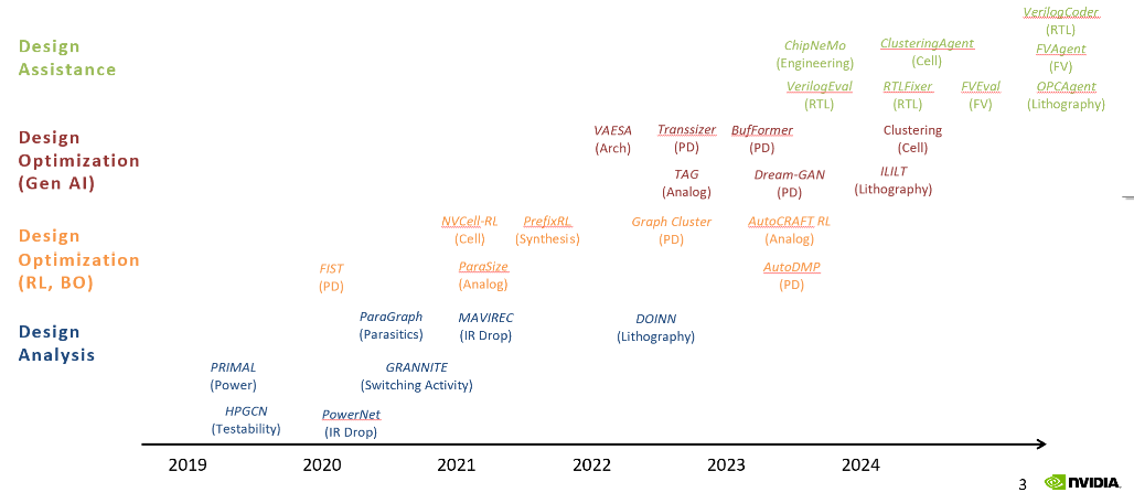
These use cases have evolved over time as shown by Nvidia in Figure 1 below. Similarly, over time, the complexity of design tasks undertaken by AI has increased. The search space for something like clock tree optimization might be on the order of 10^4 possibilities while a memory generator that considers area, static and dynamic power, latency, bandwidth, and process might consider a state space on the order of 10^25 possibilities.
 Figure 1 : Development of Analysis, Optimization and Assistance Tools at NVIDIA
Analysis
Deep Learning techniques, such as convolutional neural networks (CNN) and graph neural networks (GNN), have found effectiveness in analysis. Both techniques are applicable to large data sets, which are typical in physical layout databases or circuit netlists. For example, estimating the IR drop on a power network within a chip can be a computationally intensive task. In MAVIREC, an AI model is given a chip’s powermap and is used to estimate the IR drop in seconds versus hours by traditional EDA means.
Optimization
Computers have long been used to optimize chip designs, with traditional AI techniques employed for some optimization tasks. In Bayesian optimization, a model is used to estimate the value of an objective function and its uncertainty, with the model’s output subsequently fed into the objective function for evaluation. The ability to estimate a black-box function can be applied to various chip optimization problems. For example, in AutoDMP, an objective function aims to optimize wire length, congestion, and density for standard cell placement. In this case, Bayesian optimization techniques are used as a lower computational cost proxy for actual standard cell placement results from a commercial EDA tool.
Reinforcement Learning (RL) techniques involve using AI to generate potential implementations and provide feedback to AI tools to reinforce better solutions. The RL algorithm uses the feedback to learn the relationship between input parameters and their effect on the outcome. One example of using an RL tool is fixing design rule check (DRC) errors in physical layout. In NVCell, an RL tool learns to fix design rule violations found by a design rule checker. In the tutorial, we show an example where the tool learns to add metal 0 to a physical layout to eliminate design rule violations.
A second example employs RL to create optimal prefix adders. Prefix adders can have many design variations. Each variation might have different timing, power and area characteristics based on physical design properties (e.g. wire resistance, routability, congestion, etc). In PrefixRL, the machine replaces human intuition by generating prefix adder designs that may not have occurred to a human designer. The result is a more optimized design than well known prefix adder architectures.
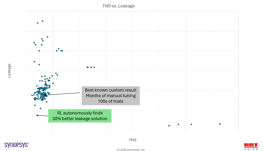
A third example using RL for chip design is optimizing power, performance, and area (PPA). In this case, RL takes into account multiple goals – Leakage, Timing, and Design Rules – and explores design options, tool selection, tool parameters, and library cell options. As shown in Figure 2, the RL AI tool achieved a better result (lower power, faster) than a hand optimized design.

Figure 2. AI-Assisted Design Search
A possible drawback of RL-based techniques is their reliance on potentially costly design evaluations. For example, assessing the effectiveness of a particular cell placement may require running various physical design tools, extracting timing, area and parasitic information to arrive at a timing, power and area cost.
Assistance
The idea behind assistance is to use AI to help engineers perform higher-level design related tasks involving high-dimensional inputs representing design tradeoffs. Calculating the “cost” of the output based on these inputs can be computationally expensive. Thus, without some estimation techniques, exploring the design space automatically may not be practical. Traditionally, human intuition, experience and high level simulation models are used to determine an “optimal” design. However, AI software can instead make estimates on which designs are more likely to approach optimality at a lower computational cost than running the actual simulations.
An example of a large design space with potentially costly evaluations is logic synthesis. After RTL elaboration, computationally expensive synthesis and place and route tools are used to evaluate the PPA of the result. In FastPASE, a graph convolutional network (GCN) is used to estimate the PPA of a given RTL design before logic synthesis. The result is a 10X improvement in evaluation speed.
Large Language Models and Chip Design
The recent popularity of Large Language Models (LLMs) has had enormous impacts on many disciplines. Since the public availability of ChatGPT and other LLMs, people have utilized them in a plethora of diverse applications. Fundamentally, LLMs are trained on sequences of text (tokens). These models try to predict subsequent tokens based on a prompt (given input pattern). To date, these models have been used with fairly high success in applications such as automatically generated software.
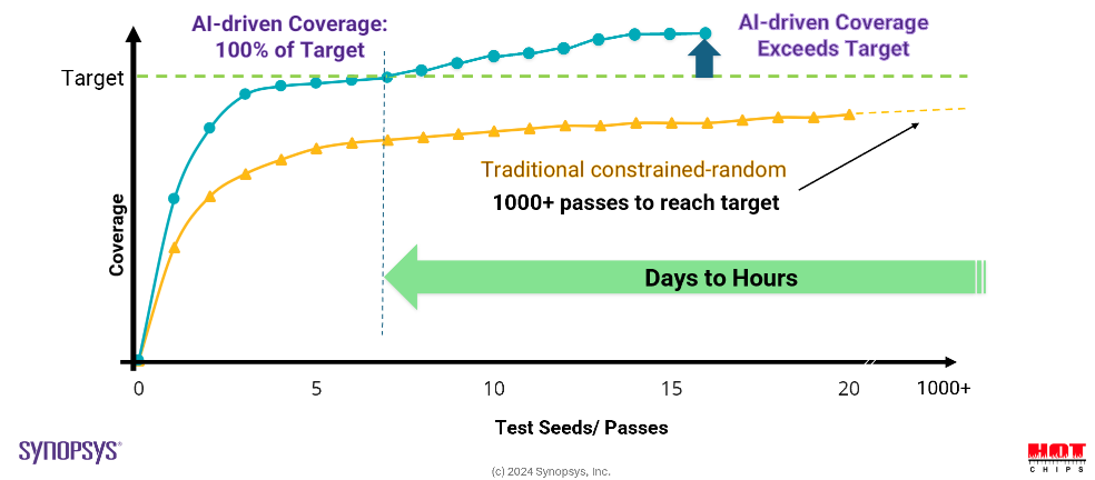
As an analog to the use of LLMs to generate software, one might also use an LLM to generate a design in a Hardware Description Language (HDL) such as System Verilog. Similar use cases include generating verification testbenches or EDA scripts. In the testbench generation use case, an LLM is used to generate constrained random tests for RTL verification. The target coverage is achieved with fewer simulations and in less time than traditional methods, as shown in Figure 3 below.

Figure 3: Enabling Faster Time to Closure
Similarly, an LLM can be used to generate scripts for EDA tools. For instance, in ChipNeMo, an LLM is tasked with generating EDA scripts to gather the number of flip-flops in a certain region of the chip and identifying logic related to a particular circuit. The designer can uses natural language prompts such as “Write a code in TOOL1 to print the number of flops in the rectangle (0, 0, 100, 100)” or “Write a TOOL2 tcl proc to find intersecting logic from ‘$pinA’ to ‘$pinB'”.
RAG (Retrieval augmented generation)
LLMs can be used to augment access to existing data. For example, complex chip design methodologies often incorporate large bug databases. An LLM can be used to generate queries to the database while not having been explicitly trained on the contents of the bug database.
RAG may also be used to read library documentation on particular RTL IP, and then generate module connections between components. For example, a user might ask a RAG model to “Propose top-level Verilog for a module connecting the AXI-APB bridge IP to the RTC IP”. The model then accesses some documentation on the AXI-APB IP and the RTC IP and generates a Verilog module interface. Note, the LLM was not specifically trained on the library but uses it as an external source.
The idea of using general LLMs in a specialized domain, such as chip design, falls under the umbrella of Domain-adaptive LLMs. In this framework, a general LLM is augmented with domain-specific knowledge. For example, an EDA vendor may provide an LLM, which has general chip design knowledge and tools for the customer to augment that model with its proprietary IP specific data. For example, in RTLFixer, an LLM accesses a database of human expert Verilog knowledge to better fix RTL syntax errors. The result is higher quality automatically generated RTL code than a one-shot approach.
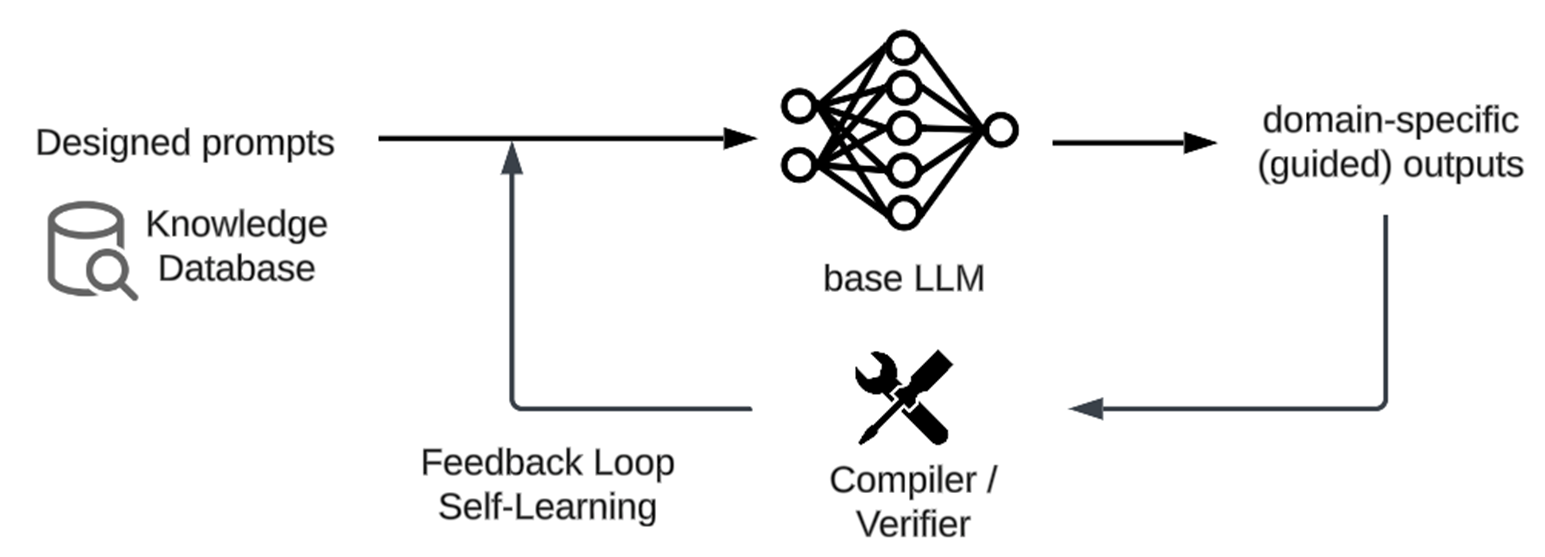
Domain-adaptive LLM techniques can be categorized based on which design stage they are employed at, whether in the model pre-training, fine-tuning, or inference stages. Incorporating large-scale domain data during the pre-training stage will create a domain-specific LLM from the ground up. Alternatively, we can instead take a base LLM and fine-tune it using task-specific domain data to adapt a general-purpose LLM to domain specific tasks. Finally, during the inference stage, domain knowledge can be fed into the model through prompt engineering, agent or RAG techniques as employed in RTLFixer. Figure 4 illustrates the process of domain-adaptive inference. Given these options, an open research question is how to choose among these domain-adaptive techniques for various chip design tasks.

Figure 4: Domain-Adaptive Inference Loop
AI Agents
As the field of using AI for chip design develops, more complex tasks become feasible with AI tools. A promising area is the use of AI agents.The basic idea of AI agents is to pool resources by incorporating multiple agents, each with perhaps different expertise. The agents may also use tools – for example, LLMs are generally not very good at math, but an LLM Agent can be taught to use a calculator to perform mathematical operations. Similarly, agents can be taught to use various EDA tools as well as interacting with other agents.
Agents at each level can be used to implement parts of this flow. In ChatDev, different agents perform different functions (CEO, CTO, Reviewer, Tester, Programmer) in the process of generating software. These agents interact with one another to perform the overall task.
A similar organization of agents can apply to chip design tasks. For instance, multiple agents can be used to generate RTL code from a high-level specification as done in VerilogCode. One agent could be responsible for high-level task planning, generating detailed task specifications such as what modules are needed, what is the function of each module, and what are the modules’ inputs and outputs. A second agent could then generate Verilog code based on these specifications. A third agent may be used to test and debug the design. All agents can make use of external tools (e.g. floorplanners, logic synthesis tools, timing tools, etc).
Closing Thoughts
The task of chip design incorporates complex tradeoffs and domain-specific knowledge. AI has been used in the past for parts of the chip design process. Recently, AI has found more applications in higher level complex tasks. The broad categories of analysis, optimization and assistance represent increasingly difficult tasks. As AI evolves, we are starting to see AI’s use in many diverse and complex chip design tasks. In this article, we only briefly described some of the areas where AI is impacting chip design. Interested readers are encouraged to visit HotChips to watch the full tutorial and access the accompanying materials (for those who did not attend the conference, the videos and materials will be made accessible to non-attendees in December 2024). Our hope is that the tutorial will motivate wider awareness of AI in chip design and inspire new ideas and applications in this field.
About the Authors:
Bryan Chin is a Continuing Lecturer in UCSD CSE department. Before his teaching career, Bryan worked for over 30 years in industry designing microprocessors around the SPARC, MIPS, Arm, x86 and PowerPC architectures. He has worked in the areas of architecture, performance, logic design, logic verification, EDA and DFT roles.
Jishen Zhao is a Professor at UCSD CSE department. Her research spans the boundaries of computer architecture, systems software and machine learning. Jishen co-authored over 80 publications in the areas of computer architecture and machine learning.
Haoxing (Mark) Ren, Mark is the Director of Design Automation Research at Nvidia. Mark has over 20 years experience in industrial research with over 100 published papers in the area of machine learning and chip design.
Stelios Diamantidis is a Distinguished Architect at Synopsys where he heads the Generative AI Center of Excellence. He led DSO.ai, one of the first AI applications for chip design. Stelios has over 25 years experience in semiconductors and EDA software.
Hans Bouwmeester is the COO at Primis.AI. His focus is in Generative AI technologies for ASIC and FPGA design and verification. Hans has over 20 years of experience in semiconductor development and related software.
Hanxian Huang is a 5th year PhD candidate at UCSD. Her research interests span the intersection of machine learning and programming languages, compilers and software/hardware systems. Hanxian was selected as one of the MLCommons Rising Stars in 2024.
Disclaimer: These posts are written by individual contributors to share their thoughts on the Computer Architecture Today blog for the benefit of the community. Any views or opinions represented in this blog are personal, belong solely to the blog author and do not represent those of ACM SIGARCH or its parent organization, ACM.


