To meet machine learning (ML) practitioners’ insatiable demand for higher processing power, computer architects have been at the forefront of developing accelerated computing solutions for ML that fundamentally changed the landscape of the computing industry. Given latest trends where application developers seek to deploy larger, deeper, and more complex deep neural network (DNN) topologies, it appears the path forward in this research domain lies in the ability to continue scaling up the performance of ML accelerators (also known as neural processing units, aka NPUs) that meets the computation demands of training emerging scale-up ML algorithms.
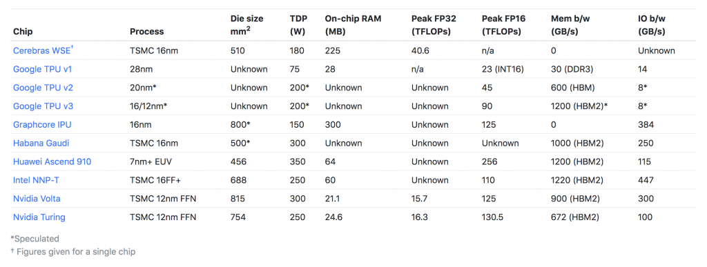
As DNN training is a throughput-limited algorithm, we are seeing both GPUs and NPUs being manufactured with a gigantic processor die size backed with bandwidth-optimized memory to maximize throughput (Figure 1). For instance, NVIDIA’s V100 already reached the reticle limits of 815 mm2 even back in 2017 and the die size of GraphCore’s IPU (2019) also reached close to 800 mm2. Google TPUs are also getting larger on successive versions of this architecture, going from 331 mm2 (v1-2016) to 648 mm2 (v3-2018). Unfortunately, transistor scaling has significantly slowed down and optics and manufacturing constraints limit the reticle size, constraining the maximum processor die size that can practically be manufactured. These trends pose challenges as to how computer architects should go about continuing to scale up the performance of NPUs that satisfies the computation demands of training next-generation ML applications.

Figure 1. Key specification of representative ML accelerators (figure from “New Chips for Machine Intelligence”)
Existing measures for performance scaling
Rather than scaling up a single ML accelerator’s chip-wide performance, an alternative solution to enhance application performance is via board-level and system-level integrations: Google’s Cloud TPU platform currently employs four TPU chips within a single PCIe board and connects multiple of these boards under the PCIe root complex. While efficient and conceptually simple to implement, multi-GPU/NPU solutions based on such board-/system-level integrations present several trade-offs. First, the end-user/ML framework/runtime system must efficiently parallelize and distribute the DNN algorithm across the multiple chips (within and across PCIe boards) optimized for the target hardware system interconnect for maximum efficiency. Second, the data movements involved in having the ML accelerators communicate and synchronize with each other dissipate significant energy over the system interconnect, deteriorating overall energy efficiency, the problem of which will become more significant as we see faster GPUs/NPUs (i.e., Amdahl’s law).
In general, the maximum possible communication bandwidth and energy/bit characteristics of these interconnect technologies become progressively worse as communication moves off-package, off-board, and off-node. Although the aforementioned integration tier is an essential component of today’s scale-out ML systems, there exist significant merits in scaling “up” a single NPU’s chip-level performance so that the communication incurred off-board and off-node gets reduced, improving both performance scalability and system-level energy-efficiency.
Wafer-scale integration for “extreme” scale-up designs
To address some of the challenges of scale-out ML systems, Cerebras at HotChips-2019 presented the ultimate scale-up NPU design — a wafer-scale ML accelerator packed with 1.2 trillion transistors and 18 GB of scratchpad memory spread across a “single” 46,255mm2 die. While the demonstration of a wafer-scale NPU prototype is certainly eye-catching, several important questions are still left unanswered (e.g., manufacturing costs, effective TOPS/Watt, cooling, TCO, …). More crucially, given how fast-evolving the ML algorithm research space has been lately (e.g., Attentions are now the de-facto standard in designing natural language processing models as opposed to the previously prevalent recurrent neural networks based seq2seq models), it remains to be seen how much performance advantage such extreme wafer-scale design will be able to deliver by the time it is actually shipped to end-users. For instance, unlike conventional ML applications for computer vision which is dominated by dense linear algebra routines (e.g., convolutions or GEMMs, a scenario where such dense-optimized wafer-scale NPU might come in handy for training), DNN-based recommendation models spend a non-trivial amount of execution time on non-DNN components such as embedding layers, which makes it less appealing to devote the entire 46,255mm2 die worth of transistors all utilized for accelerating dense computations. A previous SIGARCH article titled “The First Trillion-Transistor Chip: A New Design Space” by S. Lee provides a great summary of the details of this wafer-scale NPU design, its implications, and forthcoming technical challenges.

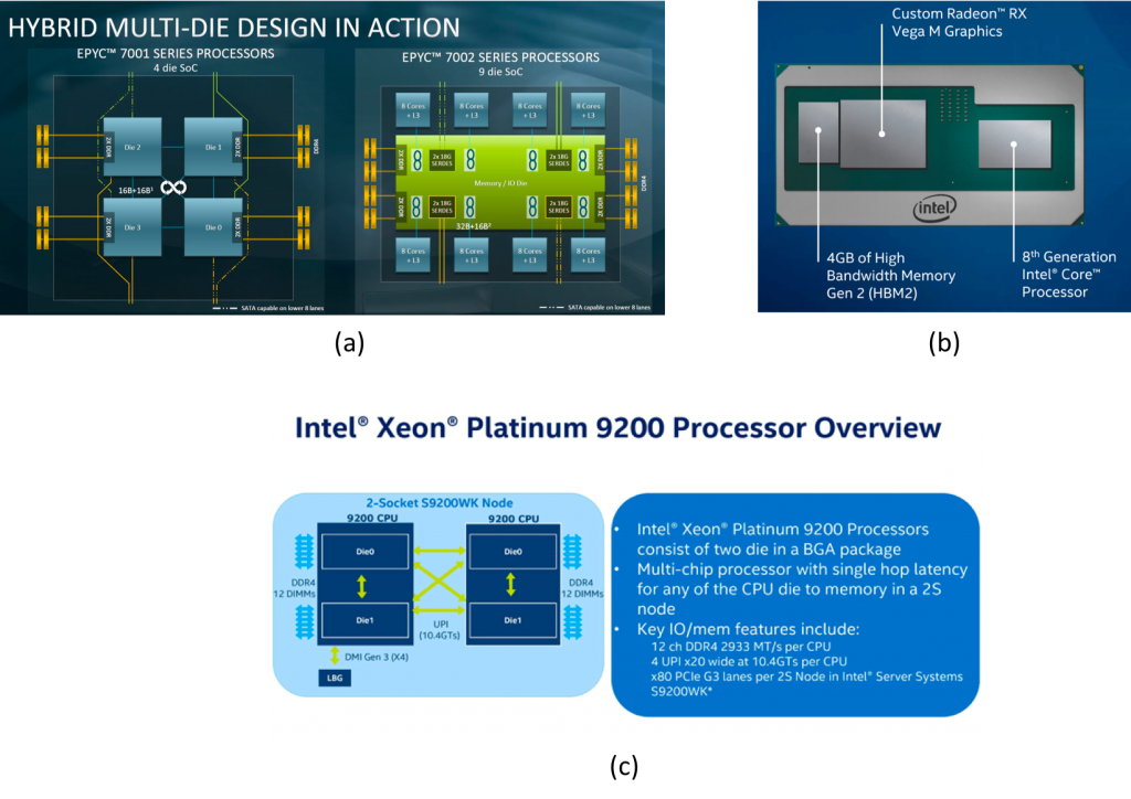
Figure 2. Recent commercialized products employing MCM technology: (a) AMD’s Epyc Rome, (b) Intel’s Core i7-8809G, and (c) Intel’s Xeon Platinum 9200.
“Package”-integrated NPUs: A New Design Space for Performance Scaling
To overcome the rising cost and yield issues of large processor packages, the chiplet model is recently gaining traction as an alternative solution to the monolithic chip design methodology. A chiplet is a block of integrated circuitry designed to work with other chiplets to form a larger and more complex chips. Under such a model, a chip designer is given a library of modular chiplets, each developed under a different process node or optimized for different functionalities. A multi-chip module (MCM) design connects multiple of these chiplets using a die-to-die interconnect and assembles them inside a larger, monolithic package using advanced packaging technologies (e.g., EMIB, Foveros 3D).
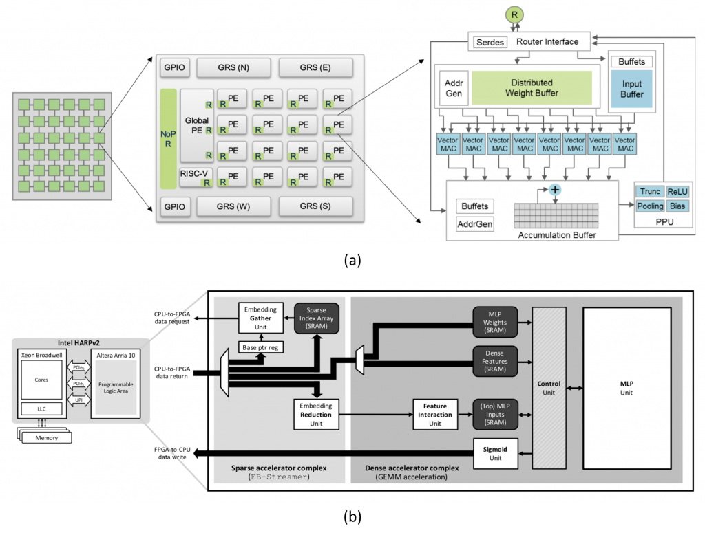
The idea of chiplets and its integration at the package-level is certainly not new. Both industry and academia have discussed such an approach for years. Only recently, however, we are seeing multiple industrial vendors rallying around such MCM model and shipping real silicon to end consumers, examples of which include AMD’s Epyc Rome and Intel’s Xeon 9200 and Core i7-8809G (Figure 2). These MCM based designs bring several technical merits than the aforementioned wafer-scale integration: process advantage, higher yield, cheaper cost, earlier time to market, the ability to mix-and-match different chiplets within the same package, etc. More importantly (and relevant to this article), the chiplet model opens up opportunities to design scale-up processor architectures for ML training using its composability while side-stepping the limitations of wafer-scale integration. Interestingly, it appears that Intel’s upcoming discrete Xe GPU (codename Ponte Vecchio), which specifically targets the high-end HPC and ML training market, is heavily employing an MCM approach. Leveraging this package-level integration tier, it appears that a chiplet-based, MCM-NPU architecture could be a promising research direction for performance scalable and composable ML accelerator design. The design space of chiplet-based NPUs is enormous and we are beginning to see interesting pursuits in this research direction within our architecture community: Simba, which integrates a “homogeneous” set of dense NPU chiplets for accelerating computer vision inference and Centaur, employing a “heterogeneous” CPU+FPGA chiplet integration approach for deploying recommendation models (Figure 3). However, the performance scalability challenge in ML training was not the primary focus in these inference-purposed accelerator designs, so it will be interesting to see what alternative research ideas and directions are most appropriate for training scenarios.

Figure 3. Chiplet-based ML accelerators (a) employing a “homogeneous” set of NPU chiplets for computer vision inference (Shao et al., “Simba: Scaling Deep-Learning Inference with Multi-Chip-Module Based Architecture”, MICRO-2019), and (b) integrating “heterogeneous” CPU+FPGA chiplets for recommendation inference (Hwang et al., “Centaur: A Chiplet-based, Hybrid Sparse-Dense Accelerator for Personalized Recommendations”, ISCA-2020).
As a summary, it seems clear that the chiplet momentum is rising rapidly with both industry and academia racing towards finding the optimal architectural solution for their respective domain of interest. A detailed discussion on what that might be for ML training workloads is beyond the scope of our discussion, but hopefully, this article can spur interesting research ideas by provoking new directions and thoughts in this exciting research space.
About the author: Minsoo Rhu is an assistant professor at the School of Electrical Engineering at KAIST (Korea Advanced Institute of Science and Technology). His current research interests include computer system architecture, machine learning accelerators, and ASIC/FPGA prototyping.
Disclaimer: These posts are written by individual contributors to share their thoughts on the Computer Architecture Today blog for the benefit of the community. Any views or opinions represented in this blog are personal, belong solely to the blog author and do not represent those of ACM SIGARCH or its parent organization, ACM.


