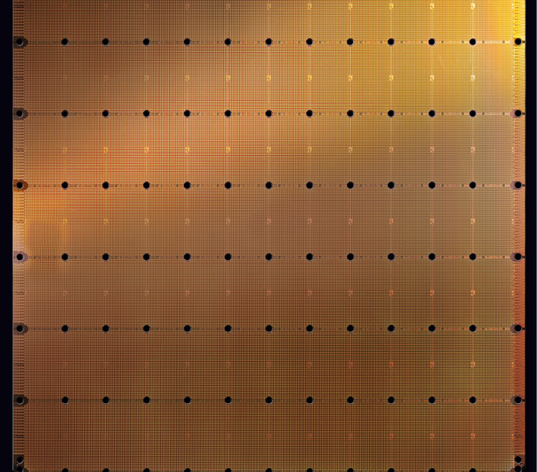
This week Cerebras announced a bold design to accelerate deep neural networks with silicon that is not cut into chips.
AI and Moore’s Law: Artificial Intelligence (AI) is much in the news for what it can do today and the promise of what it can do tomorrow (CCC/AAAI 20-Year AI Roadmap). Over half a century, AI innovation has been abetted by a million-fold progress in computer system cost-performance and parallelism. For decades, computer benefits came transparently via repeated doubling of processor performance (popularly called “Moore’s Law”). For the last decade, however, AI–especially for the great successes of Machine Learning (ML) via Deep Neural Networks (DNNs)–turned to using many general-purpose graphics processing units (GP-GPUs).
DNN Acceleration: What hardware is next for supporting AI and especially ML via DNNs? The consensus answer is: accelerators. An accelerator is a hardware component that executes a targeted computation class faster and usually with (much) less energy than general-purpose processors. In fact, GPUs are an accelerator type that have evolved to be more programmable (that’s good) but less targeted (that’s bad). Many still-emerging accelerators are hard to program directly and often present functional or performance “cliffs” to domain programmers (e.g., someone using a DNN). A well-publicized accelerator for DNNs is Google’s Tensor Processing Unit (TPU). The first-generation TPU was revealed in 2016 and programmed with the TensorFlow framework rather than directly. Subsequent TPU generations followed in 2017 and 2018 (while 2019 is not yet over).
Cerebras and Wafer-scale Integration: The latest announced entry into DNN acceleration space was presented earlier this week by Cerebras at Hot Chips 2019 (see Wall Street Journal and a white paper). This bold proposal uses a “wafer” of silicon rather than conventional “chips.” As background, silicon arrives for processing as a cylinder, is cut into 20-30 cm diameter slices called “wafers”, transistors and wires are etched onto each wafer, and traditionally the wafer is cut into rectangular chips (or die) of 0.5-6 square cm each. Cerebras eschews the final “cut into chips” step to instead do “wafer-scale integration (WSI)”. WSI holds the promise of much more capable systems, but has many costs and quality-control challenges that have kept it from being the preferred solution since Gene Amdahl advocated it at Trilogy in the 1980s.
Thus, Cerebras has placed a bold silicon bet with 1.2 trillion transistors on an area of 460 square cm (think: 8.5 inch square-ish napkin) used for 400K “cores” and 18 Gbytes of memory. On one hand, many are confident that DNNs are and will be important enough to justify the bet, and the approach facilitates efficiency gains via optimizations that cut across the software-hardware “stack”. On the other hand, there are substantial challenges. First, at and near the hardware level, Cerebras must economically address manufacturing, reliability, and cooling challenges. At the domain programmer (or even algorithm) and support software level, there must be sufficient end-to-end co-design so that the system is useful and remains useful as DNNs likely continue their amazing, disruptive advances. Exciting times!
[Editor’s Note: This post is originally from the CCC blog and is re-posted here with permission. Image source.]
About the Author: Mark D. Hill is John P. Morgridge Professor and Gene M. Amdahl Professor of Computer Sciences at the University of Wisconsin-Madison. He is the 2019 Eckert-Mauchly awardee, is a fellow of IEEE and the ACM, serves as Chair of the Computer Community Consortium (2018-20) and served as Wisconsin Computer Sciences Department Chair 2014-17.
Disclaimer: These posts are written by individual contributors to share their thoughts on the Computer Architecture Today blog for the benefit of the community. Any views or opinions represented in this blog are personal, belong solely to the blog author and do not represent those of ACM SIGARCH or its parent organization, ACM.


