Some of the most exciting applications on the horizon such as autonomous machines, Augmented/Virtual Reality, space exploration, and precision medicine rely on image sensing — at different scales. While conventional CMOS image sensors are responsible for only “imaging”, i.e., generating pixels from scene light, modern image sensors do much more: they run deep neural networks (DNNs) and buffer a large amount of data (at the order of Gb) — all in the same die! What’s fueling the ever more capable image sensors is die stacking, a technology that is perhaps more commonly seen in processor design but is virtually everywhere in high-end image sensors today.
This post discusses why die-stacked image sensors are here to stay and what they mean for algorithm and architecture design in the future.
Stacked Image Sensors
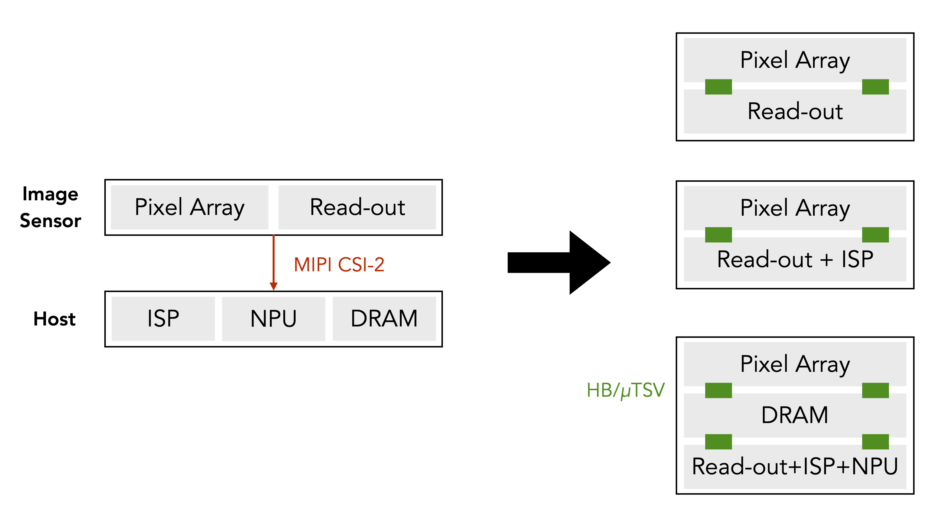
Conceptually, an image sensor has two basic components: a light-sensitive pixel array that converts photons to electric charges and the read-out logic that converts charges to digital values (RAW pixels). The RAW image pixels are transferred to the host through the MIPI CSI-2 interface to be processed by an Image Signal Processor (ISP), which removes sensing artifacts and generates clean pixels either for machines to consume (i.e., computer vision) or for humans to consume (i.e., photography).

Figure 1: (Left) Conventional image sensing system, where the pixel array and the read-out circuitry are laid out side by side in the sensor, which transfers data through the energy-hungry and slow MIPI interface to the host for downstream tasks. (Right) Different die-stacked image sensor configurations. Future image sensors will stack multiple layers consisting of memory elements and advanced computation logics. Layers are connected through hybrid bonding (HB) and/or micro through-silicon via (uTSV), which offer orders of magnitude higher bandwidth and lower energy consumption compared to MIPI.
Traditional CMOS image sensors lay the pixel array and the logic circuitry side by side. Virtually all image sensors today, however, stack the pixel array layer on top of the logic layer. Some of the early and classic examples are the SONY IMX240 sensor used in Galaxy S6 smartphones and the Samsung S5K2L2 sensor used in Galaxy S9 smartphones.
The usual advantages of die stacking, such as providing higher bandwidth and allowing for heterogeneous integration (i.e., the pixel layer and the logic layer can use their respective, optimal process node), still apply. For image sensors, however, perhaps the biggest benefit that stacking offers is the smaller form factor or, equivalently and more commonly, the ability to integrate more functionalities, mostly into the logic layer, given the same footprint.
Indeed, we are seeing a plethora of image sensors with ever more advanced processing capabilities. Below are some of my favorites.
- OmniVision (IEDM 2018): a 2-layer design where the logic layer implements Dual Conversion Gain (DCG) for low (read) noise, high dynamic range (HDR) imaging.
- Meta (IEDM 2020): a 2-layer design where the logic layer combines DCG and Time-to-Saturation mode for single-exposure HDR.
- Nikon (ISSCC 2021): a 2-layer design where the logic layer performs exposure control, key for HDR imaging, for each individual pixel tile.
- Sony (IMX 400, ISSCC 2017): a 3-layer design that integrates a pixel layer, a DRAM layer (1 Gbit), and a logic layer with an ISP. The DRAM layer buffers high-rate frames before steaming them out to the host. This enables super slow motion (960 FPS). Otherwise, the bandwidth of the MIPI CSI-2 interface limits the capturing rate of the sensor.
- Sony (ISSCC 2018): a 2-layer design where the pixel layer by default operates in the low-resolution mode; the logic layer uses frame differencing to detect moving objects on the low-resolution frames and, upon motion, signals the pixel layer to operate at the high-resolution mode and wakes up the main processor for further processing.
- Sony (IMX 500, ISSCC 2021): a 2-layer design, where the logic layer integrates an ISP for traditional image signal processing and a custom DSP for DNN processing.
I pick these six sensors as they represent two complementary uses of the extra space available in the stacked design. The first three sensors improve the fundamental imaging quality through advanced pixel circuitries. You can argue that those circuitries are better to be placed inside a sensor anyways but were not possible before due to the form factor limit. The more compact design in a stacked sensor just makes them possible. The latter three sensors, however, integrate computations, such as image signal and DNN processing, that are traditionally carried out outside an image sensor.
Moving computation into a sensor has clear advantages. Most importantly, by consuming data closer to where they are generated, we reduce the data communication energy, which, as is well recognized, dominates the overall energy consumption. Communication inside a sensor through a micro through-silicon-via (uTSV) consumes two orders of magnitude lower energy than that through the MIPI CSI-2 interface. Now imagine instead of transferring an HD image (~6 MB) we transfer only an object label (a few bytes) by running an object detection DNN inside the sensor. The savings on data transmission are more significant if the data has to be transmitted to the cloud when, for instance, the sensor itself has little to none computation capability. The energy cost of wireless communication is five orders of magnitude higher than that of uTSV.
While computations in existing stacked sensors are customized for specific tasks and will likely continue to be so, it shouldn’t be surprising if image sensors, in the very near future, integrate some form of programmable processors with an involved memory hierarchy to allow more flexible computation inside the sensor.
Two Challenges
Moving computation into an image sensor, while appealing, is not without challenges.
Thermal-Induced Noise. Performing more computation inside a sensor naturally increases the temperature. Unfortunately, image sensors are susceptible to thermal-induced noise, such as read noise and dark current noise. Recent research has shown that computation inside a sensor noticeably degrades both the perceived imaging quality and the computer vision task accuracy.
Inefficient Computation Inside Sensor. Computation inside an image sensor is inherently inefficient compared to that in the main processing chip — for two main reasons, both of which are out of cost-driven, practical considerations. First, image sensors are smaller in area than the SoC and, therefore, offer lower peak performance. Second, the process node of image sensors usually lags at least one generation behind that of the main SoC. Today, many commercial processors are fabricated using a 7 nm process node or smaller, but even high-end image sensors still use a 14 nm or 28 nm process node.
So on one hand we would like to push more computation inside the sensor to cut the data transmission volume while on the other hand the sensor also can’t do too much computation for the overhead to offset the gain. One must carefully weigh the reduction of data transmission energy against the overhead of computing inside an image sensor on a less efficient substrate.
Opportunities
Given the two limitations, the ideal workload for in-image sensor computing is one where a trivial amount of computation inside the image sensor can drastically reduce the data transmission volume. The trivial computation ensures that the thermal-induced noise is minimal and minimizes the inefficiencies of the actual computation inside the sensor.
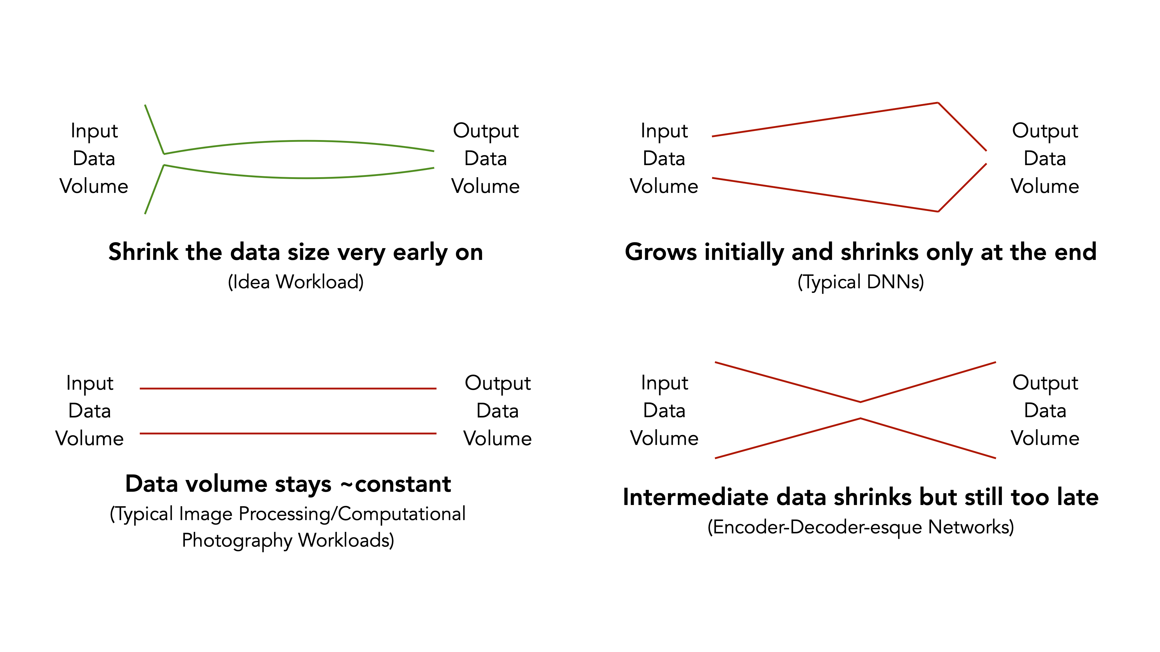
Unfortunately, many common visual computing algorithms do not fit this ideal model. The figure below compares the ideal workload model with three common workload models that are representative of today’s visual algorithms.

Figure 2: The ideal workload for in-image sensor processing (top-left) uses a trivial amount of computation in the sensor to drastically cut the data volume. Today’s typical visual algorithms (the other three panels) do not possess this characteristic.
In the ideal workload (top-left), a small amount of computation in the beginning can greatly cut the data volume, which is then transferred out of the sensor for the rest of the processing pipeline. The top-right panel represents typical CNNs, where the data volume grows initially (with lots of channels to extract features) and shrinks only at the end. The bottom-left panel represents typical image processing and computational photography algorithms, where the data volume stays roughly the same throughout the pipeline, as each processing stage takes in an image and generates another image. The bottom-right panel represents encoder-decoder-esque networks that are prevalent in domains such as medical image analysis and image synthesis. These algorithms do shrink the data volume in the beginning through the encoder/downsampling component, but the data shrinkage is not fast enough to benefit from in-image sensor processing.
Therefore, we must purposefully design new algorithms that are amenable for in-image sensor processing by construction. One such approach is to use a tiny DNN in sensor to predict and extract only the Region-of-Interests (ROI) that are relevant to the downstream tasks. On eye tracking tasks, the ROIs usually contain only one-fifth of the pixels of a full-resolution frame. Critically, for the in-sensor processing to be lightweight, the ROI-prediction DNN operates on events, which are changes in pixel brightness levels, rather than full frame pixels. Using events enables a low overhead in-sensor ROI prediction because: 1) events are naturally sparse and can be efficiently encoded, and 2) events also inherently encode the temporal changes, providing natural cues to ROI prediction.
Looking Forward
Stacked image sensors are here to stay. It’s predicted that by 2023 80% of the CMOS image sensor production will be based on the 3D stacking technology. To make effective use of the stacked sensors, however, we must address two interlocked issues: 1) what should be computed inside the sensor, and 2) how to architect the processing logic inside the sensor.
Rather than simply deciding which portion of an existing algorithm should be “offloaded” to the sensor, we must rethink algorithm design for in-image sensor processing. Apart from the in-sensor ROI prediction, many opportunities exist. For instance, instead of mitigating or reducing the thermal-induced noise, can we embrace the noise and design downstream algorithms with the noise profile in mind? In the long run, holistically designing the sensing and computing architectures will provide a greater return of investment compared to designing each individually and simply stitching them together. This co-design hinges critically on the ability to model and explore the hybrid optical-electrical-mechanical design space across performance, power, and thermal measures, as several recent work has started exploring.
About the Author: Yuhao Zhu is an Assistant Professor of Computer Science at University of Rochester. His research group focuses on applications and computer systems for visual computing.
Disclaimer: These posts are written by individual contributors to share their thoughts on the Computer Architecture Today blog for the benefit of the community. Any views or opinions represented in this blog are personal, belong solely to the blog author and do not represent those of ACM SIGARCH or its parent organization, ACM.


