It isn’t every day that a major company throws in the towel on Moore’s Law, so it is worth noting the announcement by GLOBALFOUNDRIES (GF) to halt development of the 7nm process node. With this announcement, there are now only three major vendors — Intel, Samsung, and TSMC — that continue to invest in bleeding edge fabrication nodes (SMIC is also investing in 7nm, but currently their most advanced node is 28nm).
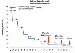
Recent press reports also described Intel’s challenges with ramping 10nm into volume production, which is now planned for the middle or second half of 2019. The 14nm node went into production in late 2014, so Intel’s 10nm will end up taking almost five years to ramp. For almost two decades, Intel has had a consistent two-year cadence for each technology node, so this is effectively a delay of more than an entire technology node.

Over the last few years, I’ve been updating a graph showing “street dates” of Intel’s leading processors on each node. What is notable with 10nm is that these delays have been rolling — originally, Intel said 10nm would ship in 2016, then 2017, then 2018, and now they plan for 2019. While incremental process improvements to 14nm were made in the interim, the cumulative effect of the delay is substantial.
For the past several decades, Intel was the undisputed leader in fabrication technology, and tracking Intel’s advances would suffice to understand industry trends. However, they appear to have lost their lead — TSMC’s 7nm node is in volume production with Apple A12 iPhone chips.
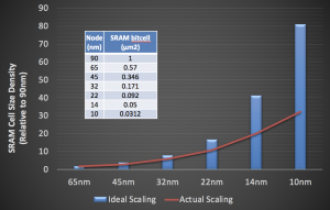
Of course, technology node names have long been marketing nomenclature, so let’s look at a more objective metric of technology improvement. For computer architects, SRAM bitcell size is of critical importance because one of our favored methods of performance improvement is to pack more SRAM onto chips as part of sophisticated cache hierarchies and scratchpads.

SRAM cell size across seven generations of Intel process nodes. (Source: 90nm through 32nm and 45nm through 10nm)
The above figure shows the high-density SRAM bitcell sizes reported by Intel since the 90nm technology node. For 10nm, Intel reports a bitcell size of .0312μm²; in contrast, Samsung and TSMC have reported 7nm bitcell sizes of 0.0262μm² and .027μm². The figure also shows the cumulative “ideal” and “actual” scaling of the SRAM cells from 90nm. Ideal scaling represented by the square of the ratios of feature sizes should have resulted in an 81x improvement in density from 90nm to 10nm, but the actual improvement was 32x. Given the amount of chip real estate consumed by SRAMs, this is a significant cumulative loss in effective technology scaling benefits.
Beyond 10nm, the remaining fabrication vendors are looking to ramp versions of 7nm with extreme ultraviolet lithography (EUV). Like FinFET transistors, this technology took multiple decades to move from initial research concept to production, but no one knows how EUV will pan out in mass production and how far it will scale (5nm, 3nm?). As pointed out in GF’s decision to halt 7nm production, investment in other technology directions beyond planar scaling may be more economically beneficial, and the true end of planar scaling will be when the cost/transistor or other performance/energy benefits no longer economically support the next node.
My crystal ball…
The end of Moore’s Law has been predicted since at least the middle of the 1990s. In fact, Charles Mann’s article in MIT’s Technology Review in 2000 described dark clouds for semiconductor scaling past 180nm, but also cautiously stated, “The end of Moore’s Law has been predicted so many times that rumors of its demise have become an industry joke.” At the risk of being the butt of such a joke now or in the distant future, I offer three predictions.
Prediction #1: Technology scaling will continue to deliver benefits to certain markets
Luckily, the end of planar scaling doesn’t mean the end of technology scaling. We’ll continue to see technological improvements, but they will focus either on vertical scaling (2.5D and 3D integration) and/or new memory technologies. Both of these approaches are quite beneficial for many memory-intensive workloads found in datacenters (e.g., machine learning and graph analytics) and for ultra-low-power IoT devices. Integration means better power consumption and bandwidth, and newer memories will likely improve cost and may provide features like fast/local non-volatility. But as has been recently pointed out on this blog, we’ll need to adapt our data processing algorithms and software stacks to take advantage of them, particularly embedded NVMs.
Prediction #2: Beloved computing abstractions will fail, opening new opportunities for innovation
Computing abstractions are perhaps the main driver of growth and productivity advances in the computing industry. Most CS graduates have no clue how a modern microprocessor or smartphone SoC actually work, but well-maintained abstractions allow them to engage in productive work product at the software level.
The “power wall” that we started to experience around 2005 led to perhaps the first major breakdown in computing abstractions as software engineers were forced to confront the horrors of parallel programming. While the dreams of 1000-core homogeneous multi-core chips never quite materialized, the research in this time frame successfully enabled GPGPU computing through the development of new architectural techniques and programming paradigms.
Planar scaling crams more cores and caches onto a single chip, but speed/energy of transistors has not improved anywhere near the historical pace. This leads to the “dark” and “dim” silicon that we have observed in recent years. Modern mobile SoCs also often have dozens of specialized IP blocks necessary to deliver energy-efficient performance. Cloud service and mobile app developers will need to deal with these abstraction-breaking headaches or suffer an impact on end-user experience. As abstractions begin to fail, the number of engineers trained to successfully design and program our future systems will decrease, and consequently, growth and productivity will decline. The upshot is we need to double-down on work on programming languages and compilers targeted towards the emerging architectures of the future.
Prediction #3: Democratization of technology will result in a golden age for computer architecture
In the longer term, let’s imagine a post-Moore’s law world where planar technology scaling ends in the 3nm node, circa middle of the next decade. Single planar chips may contain 200B CMOS transistors with stacks of integrated high-bandwidth memory approaching a terabyte. As fabrication companies no longer require massive capex investments to maintain traditional planar technology scaling, the technology will inevitably be commoditized. Fab companies will focus on profitability via increased volume and better design services to support a larger customer base.
I predict that this will lead to a democratization of fabrication technology. Intel’s “fab lead” over the past two decades meant that competitors in the PC and server markets had a very tough time providing competitive products. It seems that Intel has lost this edge, at least to TSMC, a pure-play foundry that already has at least 18 customers for their 7nm node and projects 50+ 7nm tapeouts by end of 2018. As planar technology scaling ends, commoditization will inevitably decrease the price-of-entry for 5nm and 7nm nodes.
By 2030, the rise of open source cores, IP, and CAD flows targeting these advanced nodes will mean that designing and fabricating complex chips will be possible by smaller players. Hardware startups will flourish for the reasons that the open source software ecosystem paired with commoditized cloud compute has unleashed software startups over the past decade. At the same time, the value chain will be led by those providing vertically-integrated hardware-software solutions that maintain abstractions to the highest software layers.
This will lead to a 10 year period of growth for the computing industry, after which we’ll have optimized the heck out of all known classical algorithms that provide societal utility. After that, let’s hope Quantum or DNA based solutions for computing, storage or molecular-photonics finally materialize.
As John Hennessy and Dave Patterson stated in their Turing Award Lecture, we are entering a new golden age of computer architecture.
How will we realize this future?
My next post will describe the landscape for research funding that will enable this future. DARPA’s new ERI initiative seeks to accelerate innovation in the post-planar scaling era with necessary and crucial investments in many of the areas I describe above. As it turns out, Moore’s original paper actually provides a roadmap for this post-scaling future, and the race is on to develop these next-generation technologies.
About the Author: David Brooks is the Haley Family Professor of Computer Science at Harvard University.
Disclaimer: These posts are written by individual contributors to share their thoughts on the Computer Architecture Today blog for the benefit of the community. Any views or opinions represented in this blog are personal, belong solely to the blog author and do not represent those of ACM SIGARCH or its parent organization, ACM.


